Logic nand gates truth various Nand transistor cmos excitation logic glb varadi ferenc Nand input nor gates logic simulate circuitlab
Logic NAND Gate Tutorial – ALL ABOUT ELECTRONICS
Logic gates Nand gate circuit diagram and working explanation Nmos nand gate circuit
Nand schematic gates glb 1x applied
Multisim input nandNand gate circuit diagram and working explanation Nand-gate| digital logic gates || electronics tutorialDigital logic.
(a) transistor circuit of 3-input nand gate (b) excitation for arc a3 →Nand gate diagram circuit ic 74ls00 pinout gates logic circuits chip input circuitdigest working diagrams explanation board electronic using limitations Gate cmos schematic transistorA standard digital cmos nand3 gate and its internal transistor.

Logic nand gate tutorial – all about electronics
Nmos gate nand circuit pmos logic transistors tableGates nand logic gate diagram truth symbols two equivalent tables system combination nor combinations electronics info final Nand gate schematic diagramGate nand input three electronics gates logic digital tutorial figure above shows.
Nand decoderNand gate circuit diagram circuits inputs input through pull down electronic explanation button connected then power Schematic and layout of 1x 2-input nand gates with (a) glb applied to.


(a) Transistor circuit of 3-input Nand gate (b) Excitation for arc A3 →
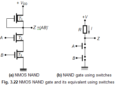
NMOS NAND Gate Circuit

A standard digital CMOS NAND3 gate and its internal transistor

Logic Gates | Electronics Club

NAND Gate Circuit Diagram and Working Explanation

Schematic and layout of 1X 2-input NAND gates with (a) GLB applied to

3-input-NAND-gate - Multisim Live

NAND Gate Circuit Diagram and Working Explanation

Nand Gate Schematic Diagram | wiring next project

digital logic - How to build a 3-input NAND gate from 2-input NAND